Download presentation
Presentation is loading. Please wait.

1
Combinational Logic 組合邏輯
Chapter 5 Combinational Logic 組合邏輯 基本的組合邏輯電路 實作組合邏輯 NAND閘和NOR閘的萬用特性 用NAND閘和NOR閘來作組合邏輯 用脈波來操作邏輯電路 檢修 可程式邏輯 數位系統應用

2
上一章的SOP邏輯表示式是用AND及OR閘來製作, 稱為AND-OR Logic.
1. 基本的組合邏輯電路 上一章的SOP邏輯表示式是用AND及OR閘來製作, 稱為AND-OR Logic. Figure An example of AND-OR logic. Open file F05-01 to verify the operation. Thomas L. Floyd Digital Fundamentals, 8e

3
例題5-1 在化工廠中有三個裝液態化學藥品的儲存槽, 每個槽 都有一個液位高度的感應器, 當某一槽的化學藥品掉到低於設
1. 基本的組合邏輯電路 例題5-1 在化工廠中有三個裝液態化學藥品的儲存槽, 每個槽 都有一個液位高度的感應器, 當某一槽的化學藥品掉到低於設 定的高度時, 該感應器就輸出高電壓. 設計一個電路來監視這 三個儲存槽, 當某兩個槽低於設定的高度時, 指示器就亮起. BC 00 01 11 10 A B C F 1 A 1 1 卡諾圖 F=BC+AC+AB BC AC AB 指示器 Thomas L. Floyd Digital Fundamentals, 8e Figure 5--2

4
POS邏輯表示式可以是AND, OR及NOT閘來製作, 稱為AND-OR-Invert Logic.
1. 基本的組合邏輯電路 POS邏輯表示式可以是AND, OR及NOT閘來製作, 稱為AND-OR-Invert Logic. Figure An AND-OR-Invert circuit produces a POS output. Open file F05-03 to verify the operation. (A+B)(C+D)=(AB)(CD)=(AB)(CD)=AB+CD=AB+CD Thomas L. Floyd Digital Fundamentals, 8e
(C+D)=(AB)(CD)=(AB)(CD)=AB+CD=AB+CD. Thomas L. Floyd Digital Fundamentals, 8e.")
5
例題5-2 若將例題5-1的感應器改用另一種形式, 即在某一槽的 化學藥品掉到低於設定的高度時, 該感應器就輸出低電壓. 設
1. 基本的組合邏輯電路 例題5-2 若將例題5-1的感應器改用另一種形式, 即在某一槽的 化學藥品掉到低於設定的高度時, 該感應器就輸出低電壓. 設 計一個電路來監視這三個儲存槽, 當某兩個槽低於設定的高度 時, 指示器就亮起. BC 00 01 11 10 A B C F 1 1 1 卡諾圖 F=B’C’+A’B’+A’C’ Figure 5 - 4 Thomas L. Floyd Digital Fundamentals, 8e

6
1. 基本的組合邏輯電路 實際的AND-OR-Invert邏輯閘
Figure A The 74LS51 dual 2-wide AND-OR-Invert and the 74LS54 single 4-wide AND-OR-Invert. The term 2-wide means there are two AND gates per device and 4-wide means there are four AND gates per device.

7
Exclusive Gate (排斥或閘) 是由兩個反向器, 兩個AND閘及 一個OR閘構成
1. 基本的組合邏輯電路 Exclusive Gate (排斥或閘) 是由兩個反向器, 兩個AND閘及 一個OR閘構成 Figure Exclusive-OR logic diagram and symbols. Open file F05-06 to verify the operation. Thomas L. Floyd Digital Fundamentals, 8e
 是由兩個反向器, 兩個AND閘及. 一個OR閘構成. Figure 5--5 Exclusive-OR logic diagram and symbols. Open file F05-06 to verify the operation. Thomas L. Floyd Digital Fundamentals, 8e.")
8
在Exclusive OR 的輸出端加一個反向器就變成Exclusive NOR
1. 基本的組合邏輯電路 在Exclusive OR 的輸出端加一個反向器就變成Exclusive NOR X = ((AB’) +(A’B))’ = (AB’)’ (A’B)’ = (A’+B)(A+B’) = AA’+A’B’+AB+BB’ = A’B’+AB Figure Two equivalent ways of implementing the exclusive-NOR. Open file F05-07 to verify the operation. Thomas L. Floyd Digital Fundamentals, 8e
 +(A’B))’ = (AB’)’ (A’B)’ = (A’+B)(A+B’) = AA’+A’B’+AB+BB’ = A’B’+AB. Figure 5--6 Two equivalent ways of implementing the exclusive-NOR. Open file F05-07 to verify the operation. Thomas L. Floyd Digital Fundamentals, 8e.")
9
Figure 5--7 Logic circuit for X = AB + CDE.
2. 實作組合邏輯 看到邏輯表示式就要知道電路長什麼樣子. Figure Logic circuit for X = AB + CDE. Thomas L. Floyd Digital Fundamentals, 8e

10
Figure 5--8 Logic circuits for X = AB(CD + EF) = ABCD + ABEF.
2. 實作組合邏輯 乘開等於右式 Figure Logic circuits for X = AB(CD + EF) = ABCD + ABEF. Thomas L. Floyd Digital Fundamentals, 8e
 = ABCD + ABEF. Thomas L. Floyd Digital Fundamentals, 8e.")
11
使用真值表畫出電路圖 A’B’C’D A’BC’D AB’C’D ABCD’

12
2. 實作組合邏輯 看到真值表,就要 能夠畫出電路圖
Figure Logic circuit for X = ABC + ABC. Open file F05-10 to verify the operation. Inputs Output Product Term A B C 1 A’BC AB’C’ 看到真值表,就要 能夠畫出電路圖 Thomas L. Floyd Digital Fundamentals, 8e

13
Figure 5--10 Open file F05-11 to verify the operation.
2. 實作組合邏輯 例題5-3 試設計可實作表5-4真值表所指定運算的邏輯電路。 Inputs Output Product Term A B C 1 A’BC AB’C ABC’ 看到真值表就要會 寫出邏輯表示式,並 畫出電路圖 X=A’BC+AB’C+ABC’ Figure Open file F05-11 to verify the operation. Thomas L. Floyd Digital Fundamentals, 8e

14
Figure 5--11 Open file F05-12 to verify the operation.
2. 實作組合邏輯 例題5-4 設計一個具 有四個輸入變數的 邏輯電路, 只有當 其中三個變數為 1 時, 輸出才為1 Figure Open file F05-12 to verify the operation. Thomas L. Floyd Digital Fundamentals, 8e

15
X = (A’B’C’)’ C + (A’B’C’)’ + D = (A+B+C) C + (A+B+C) + D
2. 實作組合邏輯 例題5-5 化簡 Figure Open file F05-13 to verify that this circuit is equivalent to the circuit in Figure 5-14. X = (A’B’C’)’ C + (A’B’C’)’ + D = (A+B+C) C + (A+B+C) + D = (A+B+C) (C+1) + D = (A+B+C) + D = A+B+C+D Figure 5--13 Thomas L. Floyd Digital Fundamentals, 8e
’ C + (A’B’C’)’ + D. = (A+B+C) C + (A+B+C) + D. = (A+B+C) (C+1) + D. = (A+B+C) + D. = A+B+C+D. Figure Thomas L. Floyd Digital Fundamentals, 8e.")
16
2. 實作組合邏輯 例題5-6 化簡 X = AB’C’ + ABC’D’ + A’B’C’D + A’B’C’D’
= AB’C’(D+D’) + ABC’D’ + A’B’C’D + A’B’C’D’ = AB’C’D + AB’C’D’ + ABC’D’ + A’B’C’D + A’B’C’D’ Figure 5--14 Thomas L. Floyd Digital Fundamentals, 8e
 + ABC’D’ + A’B’C’D + A’B’C’D’ = AB’C’D + AB’C’D’ + ABC’D’ + A’B’C’D + A’B’C’D’ Figure Thomas L. Floyd Digital Fundamentals, 8e.")
17
2. 實作組合邏輯 Figure 5--15 Thomas L. Floyd Digital Fundamentals, 8e

18
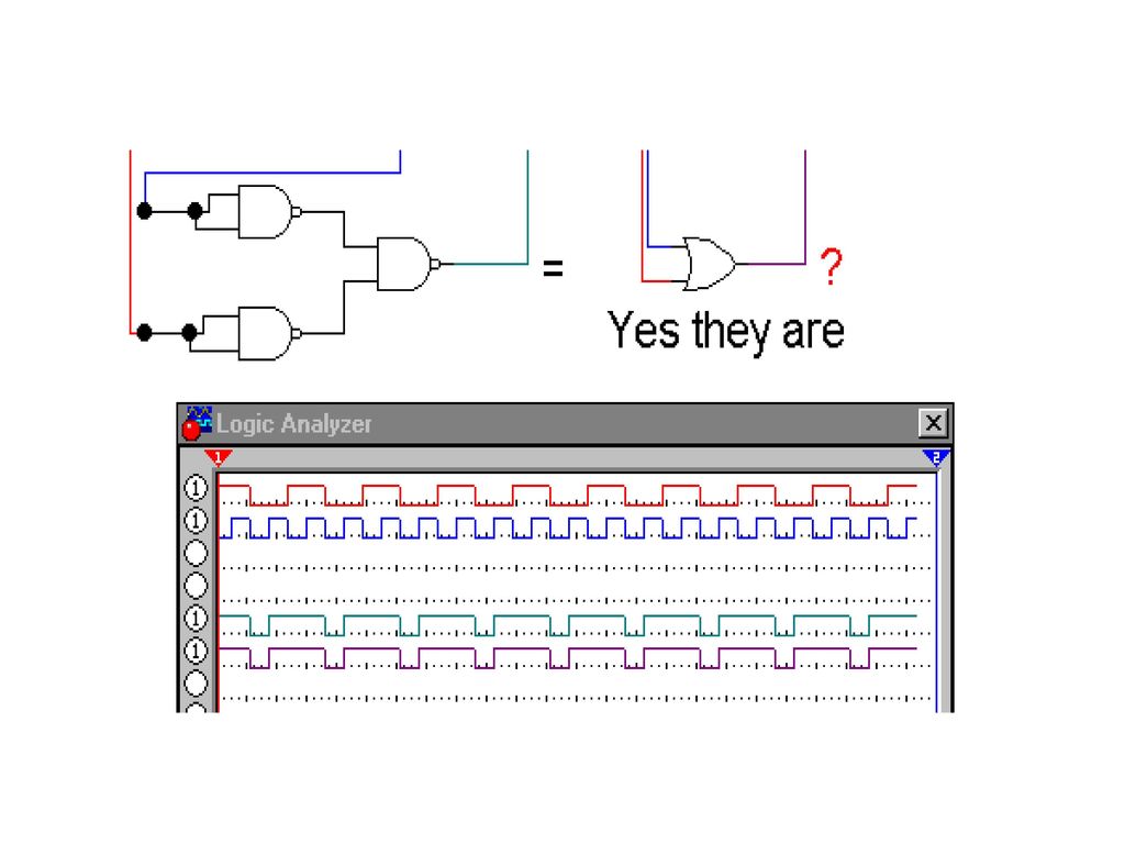
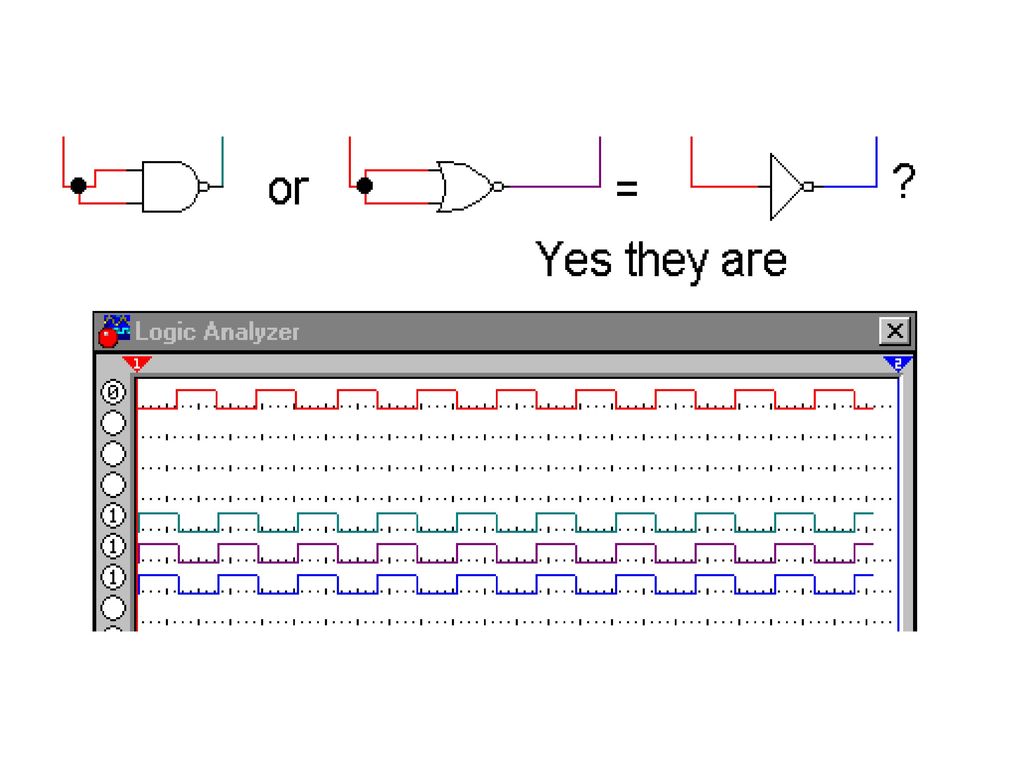
3. NAND閘和NOR閘的萬用特性 5-3 NAND閘和 NOR閘的 萬用特性
Figure Universal application of NAND gates. Open files F05-17(a), (b), (c), and (d) to verify each of the equivalencies. Thomas L. Floyd Digital Fundamentals, 8e
, (b), (c), and (d) to verify each of the equivalencies. Thomas L. Floyd Digital Fundamentals, 8e.")
19
Yes they are

21
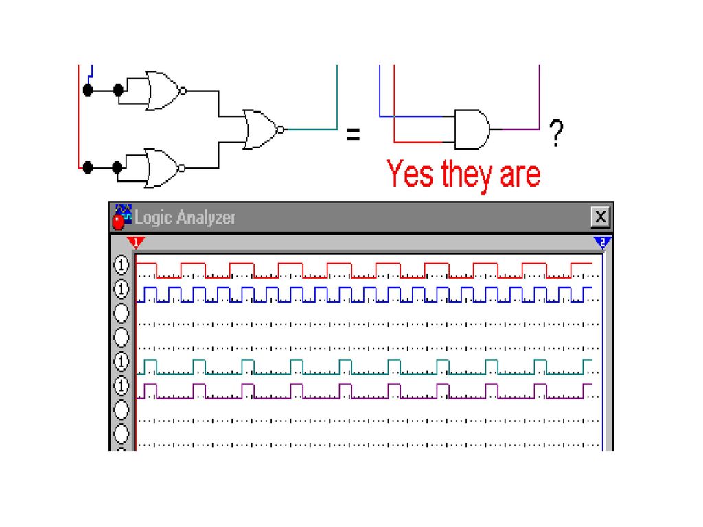
3. NAND閘和NOR閘的萬用特性 Figure Universal application of NOR gates. Open files F05-18(a), (b), (c), and (d) to verify each of the equivalencies. Thomas L. Floyd Digital Fundamentals, 8e

24
Figure 5--18 NAND logic for X = AB + CD.
4. 用NAND閘和NOR閘來作組合邏輯 5-4 用NAND閘和NOR閘來作組合邏輯 Figure NAND logic for X = AB + CD. Thomas L. Floyd Digital Fundamentals, 8e

25
4. 用NAND閘和NOR閘來作組合邏輯 Figure Development of the AND-OR equivalent of the circuit in Figure 5-19. Thomas L. Floyd Digital Fundamentals, 8e

26
4. 用NAND閘和NOR閘來作組合邏輯 Figure Illustration of the use of the appropriate dual symbols in a NAND logic diagram. Thomas L. Floyd Digital Fundamentals, 8e

27
例題5-7 使用正確的對偶符號重畫電路圖並寫出邏輯表示式
4. 用NAND閘和NOR閘來作組合邏輯 例題5-7 使用正確的對偶符號重畫電路圖並寫出邏輯表示式 Figure 5--21 Thomas L. Floyd Digital Fundamentals, 8e

28
4. 用NAND閘和NOR閘來作組合邏輯 Figure 5--22
Thomas L. Floyd Digital Fundamentals, 8e

29
例題5-8 試使用NAND邏輯閘實作下列數學式 (a)ABC+DE (b) ABC+D’+E’ SOL:
4. 用NAND閘和NOR閘來作組合邏輯 例題5-8 試使用NAND邏輯閘實作下列數學式 (a)ABC+DE (b) ABC+D’+E’ SOL: Figure 5--23 Thomas L. Floyd Digital Fundamentals, 8e
ABC+DE (b) ABC+D’+E’ SOL: Figure Thomas L. Floyd Digital Fundamentals, 8e.")
30
Figure 5--24 NOR logic for X = (A + B)(C + D).
4. 用NAND閘和NOR閘來作組合邏輯 NOR GATE Figure NOR logic for X = (A + B)(C + D). X = ((A+B)’ + (C+D)’)’ = (A+B)’’ (C+D)’’ = (A+B) (C+D) Thomas L. Floyd Digital Fundamentals, 8e
(C + D). X = ((A+B)’ + (C+D)’)’ = (A+B)’’ (C+D)’’ = (A+B) (C+D) Thomas L. Floyd Digital Fundamentals, 8e.")
31
4. 用NAND閘和NOR閘來作組合邏輯 Figure 5--25
Thomas L. Floyd Digital Fundamentals, 8e

32
4. 用NAND閘和NOR閘來作組合邏輯 Figure Illustration of the use of the appropriate dual symbols in a NOR logic diagram. Thomas L. Floyd Digital Fundamentals, 8e

33
例題5-9 使用正確的對偶符號重畫電路圖並寫出邏輯表示式
4. 用NAND閘和NOR閘來作組合邏輯 例題5-9 使用正確的對偶符號重畫電路圖並寫出邏輯表示式 Figure 5--27 Thomas L. Floyd Digital Fundamentals, 8e

34
4. 用NAND閘和NOR閘來作組合邏輯 Figure 5--28
Thomas L. Floyd Digital Fundamentals, 8e

35
二階NAND和NOR閘電路的設計 由 且應用迪摩根定律可以將一個AND和OR閘的二階電路轉換成由NAND閘或NOR閘所組成的電路。
迪摩根定律:

36
Ex:最簡積項和形式轉換成一些其它二階形式的過程。
(7-13)式、(7-14)式、(7-15)式和(7-16)式分別代表AND-OR,NAND-NAND,OR-NAND和NOR-OR形式,如圖7-11所示。
式、(7-14)式、(7-15)式和(7-16)式分別代表AND-OR,NAND-NAND,OR-NAND和NOR-OR形式,如圖7-11所示。")
37
Ex(續1):由卡諾圖可以求出F的最簡和項積形式:
(7-18)式、(7-19)式、,(7-20)式和(7-21)式分別表示OR-AND、NOR-NOR、AND-NOR和NAND-AND形式,如圖7-11所示。
式、(7-19)式、,(7-20)式和(7-21)式分別表示OR-AND、NOR-NOR、AND-NOR和NAND-AND形式,如圖7-11所示。")
38
Ex(續2):
:")
39
Ex(續3):
:")
40
多階NAND和NOR閘電路的設計 設計多階NAND閘電路的步驟: 1.化簡所要實現的交換函數。
2.設計一個多階的AND和OR閘電路。輸出閘必 須是OR閘。AND閘的輸出不能做為AND閘的 輸入,OR閘的輸出不能做為OR閘的輸入。 3.由輸出閘當作第1階開始做階層編號。以 NAND閘取代所有的閘,閘與閘之間的連接 方式保持不變。且第2、4、6...階的輸入 保持不變,而將第1、3、5....階的文字 輸入取反相。

41
多階NAND和NOR閘電路的設計(續1) 設計多階NOR閘電路的步驟: 2.設計一個多階的OR和AND閘電路。輸出閘必
1.化簡所要實現的交換函數。 2.設計一個多階的OR和AND閘電路。輸出閘必 須是AND閘。AND閘的輸出不能做為AND閘的 輸入,OR閘的輸出不能做為OR閘的輸入。 3.由輸出閘當作第1階開始做階層編號。以 NOR閘取代所有的閘,閘與閘之間的連接 方式保持不變。且第2、4、6...階的輸入 保持不變,而將第1、3、5....階的文字 輸入取反相。

42
範例:利用多階NAND閘電路實現 Sol:

43
Sol(續):
:")
44
Ex:

45
將一個AND-OR電路(即使AND和OR閘沒有交替)轉換成一個NAND或NOR電路的步驟:
AND閘轉換成NAND閘。利用在OR閘的輸入 加上反相圈圈,將所有OR閘轉換成NAND閘。 (要轉換成NOR,則要在所有OR閘的輸出以 及所有AND閘的輸入加入反相圈圈)。
。")
46
2.當一個反相輸出推動一個反相輸入時,因 為兩個反相互相抵銷,所以毋須額外的動 作。 3.當一個非反相閘輸出推動一個反相閘輸入 或相反時,則加入一個反相器使得圈圈被 消掉。(視需要選擇一個在輸入或輸出有 圈圈的反相器。) 4.當一個變數推動一個反相輸入時,則將變 數取補數(或加入一個反相器)使得補數消 掉在輸入端的反相。
 4.當一個變數推動一個反相輸入時,則將變. 數取補數(或加入一個反相器)使得補數消. 掉在輸入端的反相。")
47
Ex:

48
5. 用脈波來操作邏輯電路 5-5 用脈波來操作邏輯電路
5-5 用脈波來操作邏輯電路 例題 5-10 圖5-29電路的輸入波形A、B、C如圖所示。試決定電路的最後輸出波形X。 Figure 5--29 Thomas L. Floyd Digital Fundamentals, 8e

49
5. 用脈波來操作邏輯電路 例題 5-11 試畫出圖5-30電路的時序圖,顯示出G1、G2和 G3的各別輸出,輸入波形A和B已顯示在如圖5-30中。 Figure 5--30 Figure 5--31 Thomas L. Floyd Digital Fundamentals, 8e

50
5. 用脈波來操作邏輯電路 例題 5-12 試分析圖5-32(a)邏輯電路中每一點Y1、Y2、Y3、Y4的中間波形,再決定其輸出波形其輸入波形如圖5-32(b)所示。 Figure 5--32 Thomas L. Floyd Digital Fundamentals, 8e

51
5. 用脈波來操作邏輯電路 例題 5-13 試直接從例題5-12中圖5-32(a)電路的輸出數學式求其輸出波形 Figure 5--33
Thomas L. Floyd Digital Fundamentals, 8e

52
Troubleshooting The above circuit is built with ICs 7400 and 7402
But there is a problem.

53
The counter is counting up what is wrong?

54
X = A’B’CD’ +AB’CD’ + A’B’C’D +AB’C’D +A’B’CD +AB’CD
But X should be ABCD’+ABCD +ABC’D

55
What is wrong? Pin 2 and 3 of the 7400 chip are shorted replacing the 7400 the circuit is A B C D X X = ABCD’ + ABC’D + ABCD That is better.

56
Figure 5--35 Illustration of a node in a logic circuit.
6. 檢修 圖5-35所示這些互連的路徑共用相同的電路接點就是我們所謂的節點(node) , G1閘是用來驅動節點,而其它邏輯閘代表連接至節點的負載。 常見的錯誤型式如下: 驅動閘的輸出端開路 負載邏輯閘的輸入端開路 驅動閘的輸入端短路 負載邏輯閘的輸入端短路 Figure Illustration of a node in a logic circuit. Thomas L. Floyd Digital Fundamentals, 8e
 , G1閘是用來驅動節點,而其它邏輯閘代表連接至節點的負載。 常見的錯誤型式如下: 驅動閘的輸出端開路. 負載邏輯閘的輸入端開路. 驅動閘的輸入端短路. 負載邏輯閘的輸入端短路. Figure Illustration of a node in a logic circuit. Thomas L. Floyd Digital Fundamentals, 8e.")
57
Figure 5--36 Open output in driving gate.
6. 檢修 驅動閘的輸出端開路 Figure Open output in driving gate. Thomas L. Floyd Digital Fundamentals, 8e

58
Figure 5--37 Open input in a load gate.
6. 檢修 負載邏輯閘的輸入端開路 Figure Open input in a load gate. Thomas L. Floyd Digital Fundamentals, 8e

59
Figure 5--38 Shorted output in driving gate.
6. 檢修 驅動閘的輸出端對地短路 Figure Shorted output in driving gate. Thomas L. Floyd Digital Fundamentals, 8e

60
Figure 5--39 Shorted input in a load gate.
6. 檢修 負載邏輯閘的輸入端對地短路 Figure Shorted input in a load gate. Thomas L. Floyd Digital Fundamentals, 8e

61
6. 檢修 信號追蹤和波形分析 Figure Example of signal tracing and waveform analysis in a portion of a digital system. TP indicates test point Thomas L. Floyd Digital Fundamentals, 8e

62
6. 檢修 例題 5-14 利用波形分析找出圖5-41(a)邏輯電路故障。觀察到的波形是圖5-41(b)中綠色,紅色是正確的。
Figure 5--41 Thomas L. Floyd Digital Fundamentals, 8e

63
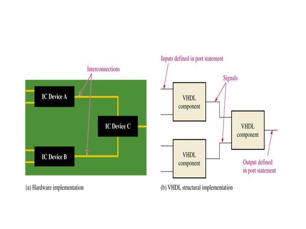
5-8 以VHDL 描述組合邏輯 運用結構描述法(Structural approach)編寫 VHDL 程式
寫VHDL程式就像將 IC元件安裝在電路板上,並用導線將它們相連接。 描述邏輯函數,並且指明它們之間如何相互連接一起。 VHDL 關鍵字component被使用在預先定義的邏輯函數。 VHDL關鍵字signal被當作以導線在元件之間進行連接的方式。

65
VHDL Components 預先定義的邏輯函數
以套件宣告(package declaration)儲存在VHDL的程式庫,並且可在程式中視需要多次呼叫。 類似一個IC的儲存盒。 任何邏輯函數的VHDL程式都可以變成元件(component) ,然後在大型程式中使用。
儲存在VHDL的程式庫,並且可在程式中視需要多次呼叫。 類似一個IC的儲存盒。 任何邏輯函數的VHDL程式都可以變成元件(component) ,然後在大型程式中使用。")
66
VHDL Components component name_of_component is port (port definition);
end component name_of_component; - 2-input XOR gate component declaration component XOR_gate is port (A, B: in bit; X: out bit); end component XOR-gate The entity XOR_gate and the architecture of the XOR_gate must also be defined
; end component XOR-gate. The entity XOR_gate and the architecture of the XOR_gate must also be defined.")
67
VHDL Signals Signals 類似於電路板上使各元件互相連接的導線。
Inputs與outputs是利用埠(Port)敘述式在實體(entity)宣告中進行宣告。 Signals 是在結構(architecture)中宣告,使用signal敘述式。 Signal是VHDL關鍵字。
敘述式在實體(entity)宣告中進行宣告。 Signals 是在結構(architecture)中宣告,使用signal敘述式。 Signal是VHDL關鍵字。")
68
Program in VHDL using structural approach

69
In a library in the entity and architecture of the OR_1 and the XOR_gate
-- program for the XOR OR circuit entity XOR_OR_Logic is port (IN1, IN2, IN3, IN4: in bit; OUT3: out bit); end entity XOR_OR_Logic;
; end entity XOR_OR_Logic;")
70
program for the XOR OR circuit continued
architecture LogicOperation of XOR_OR_Logic is component XOR_gate is port (A, B: in bit; X: out bit); end component XOR_gate; component OR_1 is port (A, B; in bit; X: out bit): end component OR_1; signal OUT1, OUT2: bit;
; end component XOR_gate; component OR_1 is. port (A, B; in bit; X: out bit): end component OR_1; signal OUT1, OUT2: bit;")
71
program for the gate XOR OR circuit continued
begin G1: XOR_gate port map (A=>IN1, B=>IN2, X=>OUT1); G2: XOR_gate port map (A=>IN3, B=>IN4, X=>OUT2); G3: OR1 port map (A=>OUT1, B=>OUT2, X=>OUT3); end architecture LogicOperation
; G2: XOR_gate port map (A=>IN3, B=>IN4, X=>OUT2); G3: OR1 port map (A=>OUT1, B=>OUT2, X=>OUT3); end architecture LogicOperation.")
72
VHDL 並行性 並行性(concurrency)表示系統可同時處理敘述式。
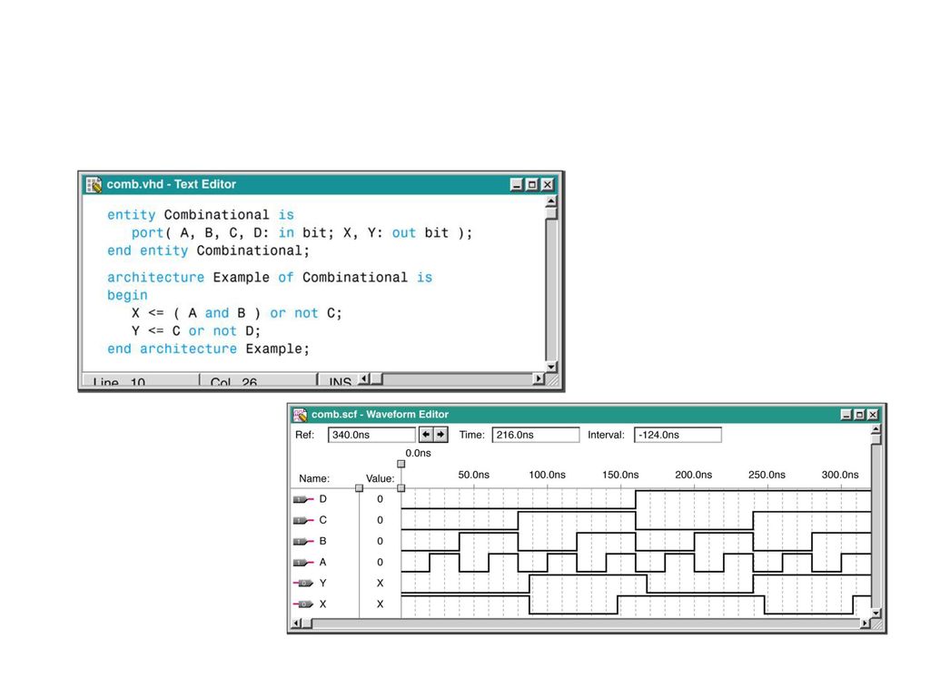
並行的概念適用於程式的架構(architecture)裡的begin和end之間的敘述式中。 entity combinational is port(A,B,C,D: in bit; X,Y: out bit) end entity combinational; architecture example of combinational is begin X<=(A and B) or not C; Y<=C or not D; end architecture example; 並行敘述式,與出現順序無關
裡的begin和end之間的敘述式中。 entity combinational is. port(A,B,C,D: in bit; X,Y: out bit) end entity combinational; architecture example of combinational is. begin. X<=(A and B) or not C; Y<=C or not D; end architecture example; 並行敘述式,與出現順序無關.")
73
VHDL Processes 過程(process)是用在程式的架構中,順序地或並行地執行敘述式。
信號串列(Sensitivity list)是過程(process) 必須處理的一組信號。 Name: process (sensitivity list) Declarations Begin Sequential statements End process;
是過程(process) 必須處理的一組信號。 Name: process (sensitivity list) Declarations. Begin. Sequential statements. End process;")
74
VHDL的變數 變數(variable)是一種可以儲存資料的物件型別 VHDL變數只能用於過程(process)中。
變數值的指定使用的是運算子 :=,如下所示: Y := B 變數宣告是放在process與begin之間。

75
例題 在飛機安全系統裡,四個液壓系統中至少要有兩個系統在整個飛行時間全速運轉,以便維持飛行安全,綠燈代表至少有一個備用系統是可以使用,紅燈代表飛機已經沒有多餘的液壓備用系統。 飛行安全系統需要邏輯1來點亮指示燈。如果液壓系統可以運轉,則它的感測器會傳回1 ;反之,會傳回邏輯0 。 試編寫一個SOP邏輯的VHDL程式碼用來監測液壓系統,如圖5-53所示。 Fig

76
我們可以寫出如下VHDL程式碼: Sol: 圖5-53邏輯圖輸出布林數學式為: X=AB+AC+AD+BC+BD+CD Y=X’
eneity flightsafety is port(A,B,C,D: in bit;X,Y: out bit); end entity flightsafety;
; end entity flightsafety;")
77
architecture sensorlogic of flightsafety is
begin poocess(A,B,C,D) variable V1:bit; V1:=(A and B) or (A and C) or (A and D) or (B and C) or (B and D) or (C and D); X:=V1; Y:=not V1; end process end architecture sensorlogic;
 variable V1:bit; V1:=(A and B) or (A and C) or (A and D) or (B and C) or. (B and D) or (C and D); X:=V1; Y:=not V1; end process. end architecture sensorlogic;")
78
運用軟體開發工具 軟體開發工具的程式碼編輯器來完成你的程式碼輸入的工作。 使用提供之模擬器測試你的程式。

80
數位系統應用 具有液面高度及溫度感應器的液體儲存槽 輸入閥 高位準感應器 警報器 低位準感應器 輸出閥 溫度感應器 加熱器
儲存槽液體數位控制邏輯 1. 控制輸入和輸出閥門 2. 控制液體溫度 輸入閥 高位準感應器 警報器 低位準感應器 控制邏輯和介面電路 輸出閥 溫度感應器 加熱器 Figure Fluid storage tank with level and temperature sensors and controls. Thomas L. Floyd Digital Fundamentals, 8e

81
操作要求 數位系統應用 當液面超過水位感測器, 感測器輸出High , 否則輸出Low 輸入閥門動作
高水位感測器為 Low, 啟動輸入閥門(High) 高水位感測器為 High, 關閉輸入閥門(Low) 輸出閥門動作(與液體溫度範圍有關) 低水位感測器為 High, 高低溫感測器為Low時, 啟動輸出閥門(High) 低水位感測器為 Low, 或高低溫感測器任一為High時, 關閉輸出閥門(Low) 加熱器(與液體溫度有關) 液體溫度過低, 低溫感測器為 High, 加熱器(H)開啟 , 否則加熱器(H)關閉' 警示鈴 當感測器故障或溫度過高, 啟動警示鈴(A) 感測器故障 當高水位感測器為High , 低水位感測器為Low ; 當兩個溫度感測器同時為High
 高水位感測器為 High, 關閉輸入閥門(Low) 輸出閥門動作(與液體溫度範圍有關) 低水位感測器為 High, 高低溫感測器為Low時, 啟動輸出閥門(High) 低水位感測器為 Low, 或高低溫感測器任一為High時, 關閉輸出閥門(Low) 加熱器(與液體溫度有關) 液體溫度過低, 低溫感測器為 High, 加熱器(H)開啟 , 否則加熱器(H)關閉 警示鈴. 當感測器故障或溫度過高, 啟動警示鈴(A) 感測器故障. 當高水位感測器為High , 低水位感測器為Low ; 當兩個溫度感測器同時為High.")
82
數位系統應用 具有液面高度及溫度感應器的液體儲存槽 表5-6 儲存槽控制邏輯的輸入和輸出 控制邏輯的輸入 變數 說明 啟動位準 備註 LH
高水位感應器 HIGH(1) 感應器侵入液體中 LL 低水位感應器 TH 高溫感應器 溫度太高 TL 低溫感應器 溫度太低 控制邏輯的輸出 VINLET 輸入閥門 閥門開啟 VOUTLET 輸出閥門 閥門關閉 H 加熱器 加熱器開啟 A 警示鈴 發生感測器故障或溫度太高的情況 表5-6 儲存槽控制邏輯的輸入和輸出
 感應器侵入液體中. LL. 低水位感應器. TH. 高溫感應器. 溫度太高. TL. 低溫感應器. 溫度太低. 控制邏輯的輸出. VINLET. 輸入閥門. 閥門開啟. VOUTLET. 輸出閥門. 閥門關閉. H. 加熱器. 加熱器開啟. A. 警示鈴. 發生感測器故障或溫度太高的情況. 表5-6 儲存槽控制邏輯的輸入和輸出.")
83
數位系統應用 表5-7 儲存槽控制邏輯的真值表 輸入 輸出 備註 LH LL TH TL VINLET VOUTLET H A 1
1 進水/加熱器關閉 進水/加熱器開啟 溫度感測器故障/警示鈴啟動 進水且排水/加熱器關閉 低水位感測器故障/警示鈴啟動 兩組感測器故障/警示鈴啟動 排水/加熱器關閉 加熱器開啟 加熱器關閉

84
數位系統應用 用卡諾圖化簡及實作輸入閥 Figure Karnaugh map simplification and implementation for the inlet valve logic. Thomas L. Floyd Digital Fundamentals, 8e

85
數位系統應用 Figure Karnaugh map simplification and implementation for the outlet valve logic. Thomas L. Floyd Digital Fundamentals, 8e

86
數位系統應用 Figure 5-- Thomas L. Floyd Digital Fundamentals, 8e

87
數位系統應用 Figure 5 IC pin diagrams.
Thomas L. Floyd Digital Fundamentals, 8e

88
數位系統應用 Figure 5 Thomas L. Floyd Digital Fundamentals, 8e

89
習題5-56 真值表 L=A’B+AB’ 房間理以電池供應能源的燈泡,由兩個開關來控制,一個在後門另一個在前門
如果前門開關(A)開啟(High)且後門開關(B)關閉(Low)或者 如果前門開關關閉(Low)且後門開關開啟(High) 則電燈(L)會亮(High) 如果兩個開關關閉(High)且兩個開關開啟(Low) 則電燈(L)會滅(Low) 真值表 A B L 1 L=A’B+AB’
開啟(High)且後門開關(B)關閉(Low)或者. 如果前門開關關閉(Low)且後門開關開啟(High) 則電燈(L)會亮(High) 如果兩個開關關閉(High)且兩個開關開啟(Low) 則電燈(L)會滅(Low) 真值表. A. B. L. 1. L=A’B+AB’")
90
End of Chapter 5

Similar presentations
.>")


 四川财经职业学院.>")


