Download presentation
Presentation is loading. Please wait.

1
数字系统设计 Digital System Design
EE141 数字系统设计 Digital System Design -----微处理器设计 王维东 Weidong Wang 浙江大学信息与电子工程学院 College of Information Science & Electronic Engineering 信息与通信工程研究所 Zhejiang University Spring ZDMC – Lec. #11

2
任课教师 王维东 TA: 浙江大学信息与电子工程学院, 信电楼306 邮箱:wdwang@zju.edu.cn
EE141 任课教师 王维东 浙江大学信息与电子工程学院, 信电楼306 College of Information Science & Electronic Engineering Zhejiang University, Hangzhou, Tel: (O) Mobile: TA: 陈彬彬 Binbin CHEN, ; 黄露 Lu HUANG, ; Tuesday & Thursday 14:00-16:30 PM Office Hours:玉泉信电楼 308室(可以微信或邮件联系). Spring ZDMC – Lec. #11
 Mobile: TA: 陈彬彬 Binbin CHEN, ; 黄露 Lu HUANG, ; Tuesday & Thursday 14:00-16:30 PM. Office Hours:玉泉信电楼 308室(可以微信或邮件联系). Spring 2016 ZDMC – Lec. #11.")
3
Prerequisites预修课程 电子电路基础 电子线路 C语言 How to learn this Course?
Not only listening, thinking and waiting …. But Exercise, Simulation, Practice!

4
课程简介 课程代码:111C0120 参考书 阎石, 数字电子技术基础, 第5版, 高等教育出版社, 2006.
EE141 课程简介 课程代码:111C0120 参考书 阎石, 数字电子技术基础, 第5版, 高等教育出版社, 2006. 王金明著,数字系统设计与Verilog HDL,电子工业出版社,第5版 补充讲义/期中考试前预备 Stanford 大学 108A课程notes. R.H.Katz, G.Borriello, Contemporary Logic Design, second edition,电子工业出版社, 2005. M.M.Mano, 数字设计(第四版), 电子工业出版社, 2010. Spring ZDMC – Lec. #11
, 电子工业出版社, Spring 2016 ZDMC – Lec. #11.")
5
Other Course Info Website: http://mypage.zju.edu.cn/wdwd/教学工作/
ftp:// /数字系统设计/2016/, 暂停 Check frequently 答疑 玉泉信电楼308室/周四下午2:30-5:00 上课课间、课后均可 ,微信群,短信均可

6
Grading (考核) Final grades will be computed approximately as follows:
期中考试-10% 课程作业+小测验+上课出勤率+Project - 20% Class Room Check Homework Sets 作业上交截止期为课后一周内有效 Project 2 projects (1 or 2 members team) Project-2可选(总评加分3~5分,但不超过平时成绩范围) Finial Exam期末闭卷考试 - 70% 上课说明此门课程的成绩合成:平时成绩包括平时小测验、期中考试、作业、出勤、课堂讨论、论文
 Project-2可选(总评加分3~5分,但不超过平时成绩范围) Finial Exam期末闭卷考试 - 70% 上课说明此门课程的成绩合成:平时成绩包括平时小测验、期中考试、作业、出勤、课堂讨论、论文.")
7
授课时间和地点: 2016年春夏学期, 地点:紫金港西1-520(多)
周二上午,第3、4节(9:50-11:25) 星期四上午,第1、2节(08:00-09:35) 地点:紫金港西1-520(多)
 星期四上午,第1、2节(08:00-09:35) 地点:紫金港西1-520(多)")
8
课程结构 数字理论知识(必备) 数字电路分析与设计 脉冲电路与接口 控制器与数字系统 微处理器简介 数字系统和编码、逻辑代数、门电路
EE141 课程结构 数字理论知识(必备) 数字系统和编码、逻辑代数、门电路 数字电路分析与设计 组合逻辑电路 触发器、半导体存贮器、可编程器件 时序逻辑电路 脉冲电路与接口 控制器与数字系统 状态机 控制器 微码控制器 测试和验证 微处理器简介 Spring ZDMC – Lec. #11
 数字系统和编码、逻辑代数、门电路. 数字电路分析与设计. 组合逻辑电路. 触发器、半导体存贮器、可编程器件. 时序逻辑电路. 脉冲电路与接口. 控制器与数字系统. 状态机. 控制器. 微码控制器. 测试和验证. 微处理器简介. Spring 2016 ZDMC – Lec. #11.")
9
讲义第十章 微处理器设计

10
以微处理器为中心的数字系统 Sensor Nets Cameras Games Set-top boxes Media Players
Laptops Servers Robots Routers Smart phones Automobiles Supercomputers

11
10.1 微处理器结构 什么是微处理器? 微处理器的主要结构 微处理器由一片或少数几片大规模集成电路组成的中央处理器。
这些电路执行控制部件和算术逻辑部件的功能。 微处理器能完成取指令、执行指令,以及与外界存储器和逻辑部件交换信息等操作,是微型计算机的运算控制部分。 微处理器的主要结构 冯诺依曼结构 将程序存储和数据存储放在同一物理存储空间 相同的总线 硬件简单 哈佛结构 将程序存储和数据存储分别放在不同的物理存储空间 不同的总线 灵活、速度快

12
冯诺依曼计算机模型 四个主要组成部分 输入、 输出、 存储器 微处理器 冯诺依曼计算机模型

13
微处理器内部结构 微处理器的两个主要部分: 控制单元 用于控制数据通路的所有操作,实现微处理器运算的正确性 数据通路
主要包括运算单元ALU、存储单元(寄存器)及其相互连接 微处理器内部结构
及其相互连接. 微处理器内部结构.")
14
指令集 专门执行一些指令集的微处理器 利用指令集编写不同的程序完成不同的处理任务 需要多少条指令集? 每条指令是什么?
每条指令的操作码(opcode)是什么? 指令编码使用多少位宽的数据? 微处理器整体结构 程序指针(Program Counter, PC)寄存器 指令寄存器(Instruction Register, IR) RISC CISC
是什么? 指令编码使用多少位宽的数据? 微处理器整体结构. 程序指针(Program Counter, PC)寄存器. 指令寄存器(Instruction Register, IR) RISC. CISC.")
15
微处理器的三个执行步骤 指令周期 (1)取指 即从程序存储器中把PC所指向的指令取出,拷贝到IR ; PC+1指向下一条指令的地址; (2)译指 从IR中提取出操作码,对指令所要做的操作进行翻译; 决定当前执行那一条指令,跳转到那一个对应的状态去; (3)执行指令 每一步将在有限状态机的一个状态被执行。 每个指令通常在一个时钟周期内执行 有些情况下一些存储器操作的指令可能需要两个甚至更长的时钟周期,这种情况下就需要更多的状态来实现正确的时序。 一般而言,程序的指令都是存储在外部寄存器中的,所以除了CPU外,微处理器一般还需要外部存储器以及连接外部存储器与CPU的地址以及数据总线。
执行指令. 每一步将在有限状态机的一个状态被执行。 每个指令通常在一个时钟周期内执行. 有些情况下一些存储器操作的指令可能需要两个甚至更长的时钟周期,这种情况下就需要更多的状态来实现正确的时序。 一般而言,程序的指令都是存储在外部寄存器中的,所以除了CPU外,微处理器一般还需要外部存储器以及连接外部存储器与CPU的地址以及数据总线。")
16
10.2 微处理器指令集 IS 指令(Instructions) 指令集(Instruction Set)
计算机语言里的单词 指令集(Instruction Set) 计算机的词汇 指令需指明要执行的操作和要使用的操作数 机器语言(Machine Language) 指令编码为二进制数格式 汇编语言(Assembly Language) 符号格式表示各种指令 基本指令 加、减和跳转指令
 计算机的词汇. 指令需指明要执行的操作和要使用的操作数. 机器语言(Machine Language) 指令编码为二进制数格式. 汇编语言(Assembly Language) 符号格式表示各种指令. 基本指令. 加、减和跳转指令.")
17
MIPS Founded by J. Hennessy
处理器指令架构ISA MIPS四个原则 (1)简洁规整; (2)加快经常性事件的速度; (3)较小的速度更快; (4)好的设计要求良好的妥协。 MIPS, Intel IA32 (x86), Sun SPARC, PowerPC, IBM 390, Intel IA64, ARM These are all ISAs RISC(Reduced Instruction Set Computer) fixed instruction length few instruction formats load/store architecture MIPS Founded by J. Hennessy (the 10th president of Stanford University, 1984) 设计ARM的原始想法完全来自于上述MIPS研究小组后来发表的论文,两位优秀并敏感的英国工程师Sophie Wilson和Steve Furber看到论文后专门跑到美国去参观实习了一把,回去后说服当时他们的公司老板开始设计ARM1,这个ARM1从1983年10月份项目启动,1年半后流片成功。 MIPS:Microprocessor without interlocked piped stages
简洁规整; (2)加快经常性事件的速度; (3)较小的速度更快; (4)好的设计要求良好的妥协。 MIPS, Intel IA32 (x86), Sun SPARC, PowerPC, IBM 390, Intel IA64, ARM. These are all ISAs. RISC(Reduced Instruction Set Computer) fixed instruction length. few instruction formats. load/store architecture. MIPS Founded by J. Hennessy. (the 10th president of Stanford University, 1984) 设计ARM的原始想法完全来自于上述MIPS研究小组后来发表的论文,两位优秀并敏感的英国工程师Sophie Wilson和Steve Furber看到论文后专门跑到美国去参观实习了一把,回去后说服当时他们的公司老板开始设计ARM1,这个ARM1从1983年10月份项目启动,1年半后流片成功。 MIPS:Microprocessor without interlocked piped stages.")
18
汇编语言 加法 减法 复杂运算

19
操作数 常数(Constants)和变量 寄存器(register) 寄存器操作 寄存器组(register set)
寄存器文件(register file) 寄存器操作 MIPS寄存器名称由$符号开头; 变量a、b和c放置在$S0、$S1和$S2; 该指令将存在$S1(b)和$S2(C)的32位值相加,32位结果写入$S0(a)。
 寄存器操作. MIPS寄存器名称由$符号开头; 变量a、b和c放置在$S0、$S1和$S2; 该指令将存在$S1(b)和$S2(C)的32位值相加,32位结果写入$S0(a)。")
20
MIPS寄存器组

21
寻址存储器指令 load word store word MIPS使用字节可寻址存储器; 存储器中的每个字节都有一个唯一的地址;

22
字节寻址组织方式 big-endian 或 little-endian方式 big-endian机器 little-endian机器
most significant byte, MSB在左侧 least significant byte, LSB于右侧 big-endian机器 字节的编号0从大(most significant)端开始 IBM 360, Motorola 68K, MIPS, SPARC little-endian机器 字节编号0从小(least significant)端开始 Intel x86, ARM, DEC Vax & Alpha,… 一个字有四个字节 字地址相同
端开始. IBM 360, Motorola 68K, MIPS, SPARC. little-endian机器. 字节编号0从小(least significant)端开始. Intel x86, ARM, DEC Vax & Alpha,… 一个字有四个字节. 字地址相同.")
23
立即数 立即数操作 立即数是一个16位二进制补码数据; 范围是[-32768,32767]
![立即数 立即数操作 立即数是一个16位二进制补码数据; 范围是[-32768,32767]](http://slidesplayer.com/slide/11627102/62/images/23/%E7%AB%8B%E5%8D%B3%E6%95%B0+%E7%AB%8B%E5%8D%B3%E6%95%B0%E6%93%8D%E4%BD%9C+%E7%AB%8B%E5%8D%B3%E6%95%B0%E6%98%AF%E4%B8%80%E4%B8%AA16%E4%BD%8D%E4%BA%8C%E8%BF%9B%E5%88%B6%E8%A1%A5%E7%A0%81%E6%95%B0%E6%8D%AE%EF%BC%9B+%E8%8C%83%E5%9B%B4%E6%98%AF%5B-32768%EF%BC%8C32767%5D.jpg "立即数 立即数操作 立即数是一个16位二进制补码数据; 范围是[-32768,32767]")
24
mips指令格式 1)R型------三个寄存器操作数格式 2)I型--------两个寄存器操作数格式 3)J型-------无寄存器格式
用于如add和sub指令,有三个寄存器操作数。 2)I型 两个寄存器操作数格式 用于如lw和sw指令,具有两个寄存器操作数和一个16位立即数。 3)J型 无寄存器格式 有一个26位的立即数,无寄存器。 MIPS采用32位指令
I型 两个寄存器操作数格式. 用于如lw和sw指令,具有两个寄存器操作数和一个16位立即数。 3)J型 无寄存器格式. 有一个26位的立即数,无寄存器。 MIPS采用32位指令.")
25
机器语言(machine language)
R-type Instructions R型是寄存器类型(register-type)的缩写 32位指令 六个数字域 op,(也称为opcode或操作码),所有的R型指令的opcode为0; rs,rt,源寄存器 rd,目标寄存器 shamt,只用于移位操作,其它R型指令,shamt为0。 funct,(也称为功能码),确定特定的R型操作 每个字段为五或六比特;
的缩写. 32位指令. 六个数字域. op,(也称为opcode或操作码),所有的R型指令的opcode为0; rs,rt,源寄存器. rd,目标寄存器. shamt,只用于移位操作,其它R型指令,shamt为0。 funct,(也称为功能码),确定特定的R型操作. 每个字段为五或六比特;")
26
R型指令机器码 R型指令add和sub的机器码 汇编指令add $S0, $S1, $ S2 RS=$ S1(17),源数据
RT=$ S2(18),源数据 结果存到 RD=$ S0(16)。
,源数据. 结果存到 RD=$ S0(16)。")
27
I-Type Instructions 名字I型是立即数类型(immediate-type)的缩写 四个字段 op, rs,源操作数
rt,如addi和lw用作目标操作数,sw作为另一种源操作数; imm,源操作立即数; rs和imm始终用作源操作数

28
I 型指令机器码 I型指令有一个16位的立即数字段, 但立即数是在32位操作中使用的。
例如,lw需要在32位的基址寄存器加一个16位的偏移量。 符号扩展 如果是正的立即数,16位立即数扩展为32位,上半部分全为0; 如果是负的立即数,扩展为32位时上半部分全为1。 2的补数符号的扩展不改变它的值。

29
Signed & Unsigned Number
If given b[n-1:0] in a register or in memory Unsigned value Signed value (2’s complement)
")
30
J-type Instructions 名字J型是跳转型(jump-type)的缩写 此格式只用跳转指令使用。
用单26位的地址操作数,addr 用于指定一个地址

31
例 将下面的机器语言代码翻译为汇编语言 0x2237FFF1 0x02F34022 把每一条指令写成二进制,
在最高六位查找每个指令的opcode,opcode决定如何解释其余位。 opcode分别为 (810)表示addi和 (010)表示R型指令, R型指令的funct字段是 (3410),这表明它是一个sub指令。
表示addi和 (010)表示R型指令, R型指令的funct字段是 (3410),这表明它是一个sub指令。")
32
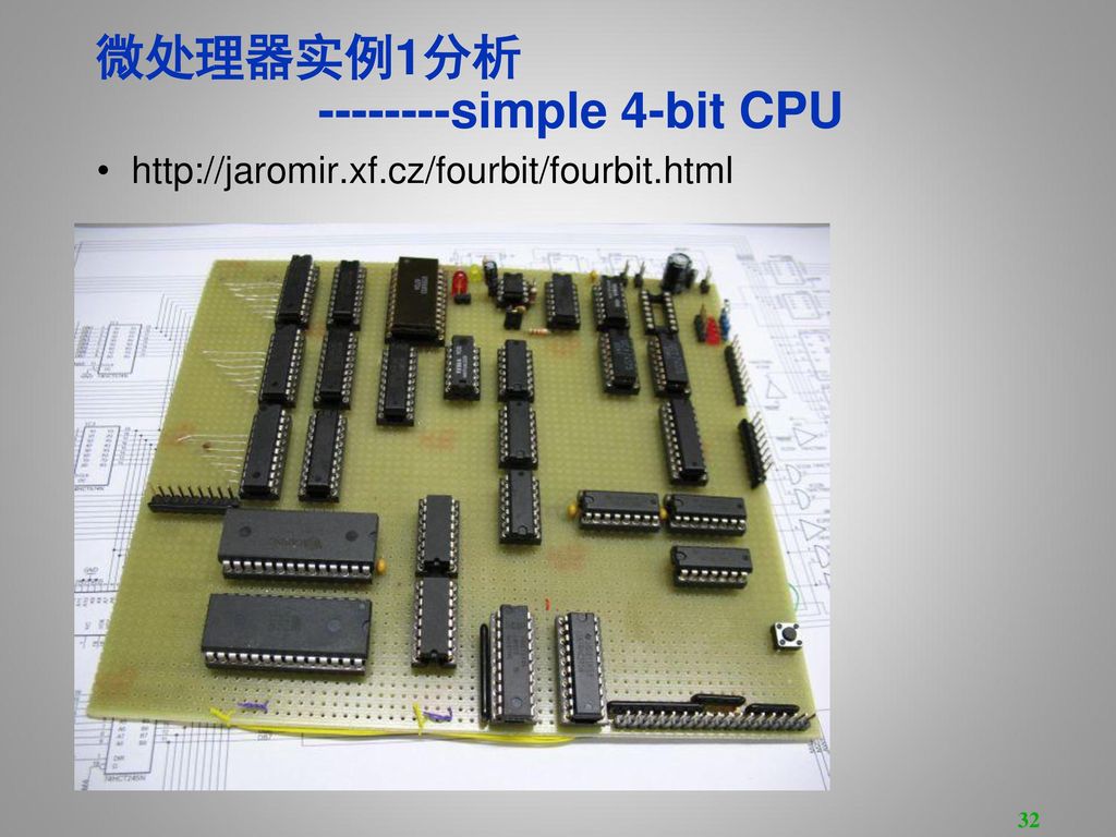
微处理器实例1分析 --------simple 4-bit CPU
33
CPU design CPU does simple things moving data from/to memory locations
making operations on it Program flow should be allowed to change IO latches are needed for real world operation

34
Registers Registers 是处理器的基本部件.
They serve as most used and useful memory locations, source or target of most of instructions. 74HCT574是8位锁存器latch,它在WE信号的上升沿从数据总线 DB锁存数据. 利用总线驱动器74HCT245,这个数据能在 OE控制下返回到DB总线. We can have a lot of registers on single bus, with WE and OE signals for each one register.

35
ALU 74LS181是4-bit wide ALU 能执行所有常用的logical和arithmetic运算.
Let's put two registers together, add and serve with single bus driver. We have two registers (A and B), ALU, with operation controlled by signals on M and S1 to S4 signals controlled by respective OE and WE signals Because 74LS181 doesn't have tristate outputs for connecting to DB, bus driver is needed here So, data in both registers (accessible from DB) can be passed through ALU and put on DB again.
, ALU, with operation controlled by signals on M and S1 to S4 signals. controlled by respective OE and WE signals. Because 74LS181 doesn t have tristate outputs for connecting to DB, bus driver is needed here. So, data in both registers (accessible from DB) can be passed through ALU and put on DB again.")
36
ALU实现的功能 要实现:一个数据放在A,另一个数据到B, 执行 ALU运算,再把结果放到 A.
需要把A数据放到bus, 变高再变低AWE(锁存),然后把B数据放到bus,变高再变低BWE. 同时, ALU执行运算(它是组合电路),结果在F1 to F4输出. 我们需要变高ALUOE,结果输出到bus. 如果要写到A寄存器, 需要变高AWE... but wait. 如果我们变高WE, 锁存的数据(ALU result)出现在A register的数据线, ALU的输出也改变了,又传输到A寄存器. 所以我们需要第三个register,叫做T - temporary register. ALU内容输出到bus:先写到T register然后再 (when ALU output is securely saved)到A register.
,然后把B数据放到bus,变高再变低BWE. 同时, ALU执行运算(它是组合电路),结果在F1 to F4输出. 我们需要变高ALUOE,结果输出到bus. 如果要写到A寄存器, 需要变高AWE... but wait. 如果我们变高WE, 锁存的数据(ALU result)出现在A register的数据线, ALU的输出也改变了,又传输到A寄存器. 所以我们需要第三个register,叫做T - temporary register. ALU内容输出到bus:先写到T register然后再 (when ALU output is securely saved)到A register.")
37
T - register Load and Store
M2: load source data from bus to T register M3=/M1: put data from T register on DB T-register

38
PC program counter – PC It's main job is to increment whenever new instruction is needed or set to value when program jump is to be made. 两个级联74HCT193计数器, EEPROM存储器放着program 和 instruction register (IR). 它存放当前instruction byte直到全部被执行. 计数器的预置输入(A, B, C and D)连到BD, 为了允许直接改变PC (program jump). 否则 PC在每个single instruction之后才改变(+1), by CLOCK UP signal (pin 5).
. 它存放当前instruction byte直到全部被执行. 计数器的预置输入(A, B, C and D)连到BD, 为了允许直接改变PC (program jump). 否则 PC在每个single instruction之后才改变(+1), by CLOCK UP signal (pin 5).")
39
Instruction decoder, part one
PC and registers with ALU are muscles of CPU, doing hard work, but it needs a brain to decide when and how to change control signals. Instruction decoder does this job. Now starts the real fun and messing with 74xx logic. Before actually building instruction decoder, it is necessary to decide which instructions we are going to decode.

40
Instructions For this computer, I decided to use only three instructions: 1, load direct data to A 2, move data from source to destination. Source can be A, B, RAM or input registers; destination can be A, B, PC, RAM or output registers. 3, do ALU operation between A and B, move result to A Allowing PC to be result of move allows jumps. You can transfer input data from IO port to RAM in single instruction. RAM is treated as another register, with address bus connected to B register. So, B is address pointer for RAM operation. Some move instructions have to affect on registers or memory. Example is move A to A. This could be equivalent of NOP instruction. There is no dedicated indirect addressing register, no stack, no interrupts.

41
Instructions MSB of instruction determines whether instruction is LDI.
We need to waste only one bit for this, so 7 bits are used as immediate data. As immediate data are one of sources for jump instructions, this allows addressing 128B of program ROM. In fact, data from ALU (computed jump) can be used for jumping but this address is only 4 bits wide, allowing addressing 16B of ROM, leaving this option as not very useful. If MSB is zero, next bit determines MOV or ALU instruction notice how this step by step description determines real operation of instruction decoder.
 can be used for jumping. but this address is only 4 bits wide, allowing addressing 16B of ROM, leaving this option as not very useful. If MSB is zero, next bit determines MOV or ALU instruction. notice how this step by step description determines real operation of instruction decoder.")
42
Instruction timing Instructions are divided into single steps. In our case, we will have for steps, let's call it machine cycles. M1: load instruction to IR and put source data on DB M2: load source data from bus to T register M3: put data from T register on DB M4: load data from DB to destination, increment PC CLK M1 M2 M3 M4 黑色方块表示active (高) 电平. CLK是输入时钟信号. 全指令做完需要eight cycles.
 电平. CLK是输入时钟信号. 全指令做完需要eight cycles.")
43
Instruction set Instruction set is simple: 7 6 5 4 3 2 1 MOVI
MOVI IMMEDIATE DATA MOV SRC DST ALU X M S3 S2 S1 S0 If 实际指令是MOVI, 源数据是 lower 7 bits from IR, 目标destination is A If实际指令是MOV,源数据是 determined by IR[3..5] and目标destination by IR[0..2] If实际指令是ALU,源数据是from ALU bus driver,目标destination is A This gives us first clue about instruction register operation. Notice 前沿of M2 comes while M1 is still high. This 重叠 is needed to 安全写数据到 T register. 同样for M3 and M4.

44
CLOCK 555时钟电路很简单. We need D-flip-flop, 除以2, 使clock有4个可能的状态.
Those states 解码by simple AND logic. To achieve 1:1 duty cycle of incoming clock signal from 555 timer, second D-FF is used.

45
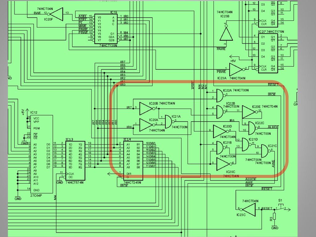
Instruction decoder, part two
Knowing what a how to decode, we can proceed in design of instruction decoder. Let‘s最复杂的instruction开始, MOV. 我们需要选择源register during phase M1 and put on bus so OE signal of 选中的 register要有效during M1 phase. 我们可以使用74HCT138 1-of-8译码器. Fortunately它有3个芯片选择脚, 2个是反向的. 连接those two 到 IR[7] and IR[6] signals, 这样在 MOV instruction时有效. Third, high active, select pin is connected to M1 signal. The same goes for selecting destination register, with the exception that third chip select pin goes to M4 signal.

46
Instruction decoder MOV instruction IC18 for SRC IC19 for DST 7 6 5 4
IR[5:3]=000 /AOE IR[5:3]=001 /BOE IR[5:3]=011 /MOE IR[5:3]=100 /IAOE IR[5:3]=101 /IBOE IC19 for DST IR[2:0]=000/ASEL IR[2:0]=001/BSEL IR[2:0]=010/PL IR[2:0]=011/MWE IR[2:0]=100/PAWF IR[2:0]=101/PBWF 7 6 5 4 3 2 1 MOVI IMMEDIATE DATA MOV SRC DST ALU X M S3 S2 S1 S0

47
Instruction decoder 为了完成MOV instruction, 我们需要小心对待T register.
OE of T register will be active during M3 and WE during M2. MOVI and ALU instructions are very alike except of that first one select IROE signal, while former selects ALUOE signal during M1. AWE (write to A register) is active during M4 for both instructions. 7 6 5 4 3 2 1 MOVI IMMEDIATE DATA MOV SRC DST ALU X M S3 S2 S1 S0
 is active during M4 for both instructions MOVI. IMMEDIATE DATA. MOV. SRC. DST. ALU. X. M. S3. S2. S1. S0.")
48
Instruction decoder IC20, IC21 and IC22 does this job
generates IROE and ALUOE signals, as well as AWE signal. For this purpose I used simple looking, but useful software, Logic Friday. I generated this truth table for AWE signal

49
Decoder circuit of logic gates
and software minimized this table into equations and generated circuit of logic gates doing the same job.

50
Decoder circuit I did the same for IROE and ALUOE signals.
Voila, instruction decoder is done. We need to make jumps conditional in some way. I decided to use register B for this purpose. When it's content is 0xF, jump (MOV to PC) is executed as NOP. Notice, on final schematics, signal M3 is not used at all. It is needed for latching output of T register, but M1 is used, as driver expects negative logic and M3 is only inverted M1.
 is executed as NOP. Notice, on final schematics, signal M3 is not used at all. It is needed for latching output of T register, but M1 is used, as driver expects negative logic and M3 is only inverted M1.")
52
Data Memory B register to Address Data IO to DB
M1: put source data on DB M2: load source data from bus to T register M3: put data from T register on DB M4: load data from DB to destination Data memory

53
Input/output ports The only thing not described for now is IO part.
We have two signals from 138 decoders, so all is needed is double 4-bit bus driver (IC25) for input ports and two 4-bit wide latches as output ports (IC26, IC27).
 for input ports and two 4-bit wide latches as output ports (IC26, IC27).")
54
ALL SCHEMATIC

55
Address A=000; 寄存器地址 B=001; IA=100; 外部输入 IB=101; MEM=011;存储器访问
PA=100; 外部输出 PB=101; PC=010; 程序地址(指针)
")
56
Programming As our CPU is basically done, we need to program it to make something useful. Lets start with simple program - emulation of four NAND gates. MOV IA,A 0b ; move data from input A to register A MOV IB,B 0b ; move data from input B to register B ALU NAND 0b ; do NAND operation {not(A&B)A} MOV A,PA 0b ; move data from A (ALU result) to port A MOVI 0b ; move zero to A MOV A,B 0b ; move this zero to B MOV A, PC 0b ; jump to zero 7 6 5 4 3 2 1 MOVI IMMEDIATE DATA MOV SRC DST ALU X M S3 S2 S1 S0
A} MOV A,PA 0b ; move data from A (ALU result) to port A. MOVI 0 0b ; move zero to A. MOV A,B 0b ; move this zero to B. MOV A, PC 0b ; jump to zero MOVI. IMMEDIATE DATA. MOV. SRC. DST. ALU. X. M. S3. S2. S1. S0.")
57
Assembly Quick hand assembly gives this output 0x20 0x29 0x54 0x04

58
Burning烧录代码 That is ready to be burned into EEPROM.
I used Genius G540 programmer really low cost, but it does its job.

59
Result, or 7400^2 to 7400^x Circuit was built on perfboard with dimension cca 18x18cm. Current consumption is about 180mA, majority of this is drawn by and in plain old TTL technology. Clock speed is determined by C1 capacitor. For 1uF, clock generator ticks at about 80Hz, giving 10Hz execution speed. For no capacitor, oscillator works at frequency given by stray capacitance, resulting in cca 57kHz execution speed. Yes, whopping 57,000 instructions per second.

60
微处理器完整电路 数据通路、控制单元电路(控制和状态信号)
")
61
Another 4-bit TTL CPU

62
The Reduced Instruction Set -APOLLO181
only 2^4 = 16 operation codes (or op-codes) Each instruction then takes an argument of 4-bit data as immediate operand Notes for the 4-bit immediate operands: § "n" is a 4-bit binary data § "r" points one of the 16 registers § "p" is a binary operand which refers to the four function–select lines (S0, S1, S2, S3) of the ALU it includes Addition, Subtraction, Shift operand, Magnitude Comparison plus twelve other Arithmetic operations. Then it includes Exclusive-OR, Comparator, AND, NAND, OR, NOR plus ten other Logic Operations § "s" can only take the binary values of “0000” (0 Hex) or “1111” (F Hex)
 Each instruction then takes an argument of 4-bit data as immediate operand. Notes for the 4-bit immediate operands: § n is a 4-bit binary data. § r points one of the 16 registers. § p is a binary operand which refers to the four function–select lines (S0, S1, S2, S3) of the ALU. it includes Addition, Subtraction, Shift operand, Magnitude Comparison plus twelve other Arithmetic operations. Then it includes Exclusive-OR, Comparator, AND, NAND, OR, NOR plus ten other Logic Operations. § s can only take the binary values of 0000 (0 Hex) or 1111 (F Hex)")
63
New Instruction set Instruction OpCode Summary Description 0000 0001
LOAD (Mem) 0000 Accum = mem[Operand]; Load data to the accumulator from a value held in RAM with the address set by the operand. LOAD (Value) 0001 Accum = Operand; Load the operand data to the accumulaor. ADD (Mem) 0010 Accum += mem[Operand]; Add value held in memory to the accumuator ADD (Value) 0011 Accum += Operand; Add operand to the accumuator SUB (Mem) 0100 Accum -= mem[Operand]; Subtract value held in memory from the accumuator SUB (Value) 0101 Accum -= Operand; Subtract operand from the accumuator STO (Mem) 0110 mem[mem[Operand]] = Accum; Store accumulator's value to memory, address held in memory. STO (Value) 0111 mem[Operand] = Accum; Store accumulator's value to memory, operand equals address. READ (Mem) 1000 Addr = mem[Operand]; Read from address, address held in memory. READ (Value) 1001 Addr = Operand; Read from address, operand equals address. JMPLOW (Mem) 1010 PC Low Addr = mem[Operand] Jump the lower 4-bits of the Program Counter to an address held in memory. JMPLOW (Value) 1011 PC Low Addr = Operand Jump the lower 4-bits of the Program Counter to an address held by the operand. JMPHIGH (Mem) 1100 PC High Addr = mem[Operand] Jump the upper 4-bits of the Program Counter to an address held in memory. JMPHIGH (Value) 1101 PC High Addr = Operand Jump the upper 4-bits of the Program Counter to an address held by the operand. JMPZERO (Mem) 1110 if(Accum == 0) { PC = mem[Operand]; } If accumulator equals zero, program counter address equals a value in program memory. JMPZERO (Value) 1111 if(Accum == 0) { PC = Operand; } If accumulator equals zero, program counter address equals the operand.
 Accum = mem[Operand]; Load data to the accumulator from a value held in RAM with the address set by the operand. LOAD (Value) Accum = Operand; Load the operand data to the accumulaor. ADD (Mem) Accum += mem[Operand]; Add value held in memory to the accumuator. ADD (Value) Accum += Operand; Add operand to the accumuator SUB (Mem) Accum -= mem[Operand]; Subtract value held in memory from the accumuator SUB (Value) Accum -= Operand; Subtract operand from the accumuator STO (Mem) mem[mem[Operand]] = Accum; Store accumulator s value to memory, address held in memory. STO (Value) mem[Operand] = Accum; Store accumulator s value to memory, operand equals address. READ (Mem) Addr = mem[Operand]; Read from address, address held in memory. READ (Value) Addr = Operand; Read from address, operand equals address. JMPLOW (Mem) PC Low Addr = mem[Operand] Jump the lower 4-bits of the Program Counter to an address held in memory. JMPLOW (Value) PC Low Addr = Operand. Jump the lower 4-bits of the Program Counter to an address held by the operand. JMPHIGH (Mem) PC High Addr = mem[Operand] Jump the upper 4-bits of the Program Counter to an address held in memory. JMPHIGH (Value) PC High Addr = Operand Jump the upper 4-bits of the Program Counter to an address held by the operand. JMPZERO (Mem) if(Accum == 0) { PC = mem[Operand]; } If accumulator equals zero, program counter address equals a value in program memory. JMPZERO (Value) if(Accum == 0) { PC = Operand; } If accumulator equals zero, program counter address equals the operand.")
64
New Instruction set The Math (Command #4, #5, #6, #7, #8, #9)
Move data inside and outside (Command #1, #2, #3, #E, #F) Comparison and Jump (Command #0, #A, #B, #C, #D)
 Comparison and Jump (Command #0, #A, #B, #C, #D)")
65
Microcode The op-code of the instruction is decoded immediately by the ROM (74188) because the most significant data-outputs of the RAM are hard-wired to the ROM addresses. For each op-code the ROM provides a microprogrammed sequence of four states. Sixteen different op-codes with four states each make sixty-four possible combinations. Thus four ROM are tied together to form a larger array of memory that consists of 64 words.
 because the most significant data-outputs of the RAM are hard-wired to the ROM addresses. For each op-code the ROM provides a microprogrammed sequence of four states. Sixteen different op-codes with four states each make sixty-four possible combinations. Thus four ROM are tied together to form a larger array of memory that consists of 64 words.")
66
Schematic for microcode

67
4 bit CPU - Micro-instruction microcode detail
ADDRESS ROM 0 ROM 1 FF 1 7F 2 BF 3 4 FD 5 DF 6 7 8 FB 9 10 11 12 13 14 15 16 17 EF 18 19 20 21 F7 22 23 24 25 26 27 28 29 FE 30 31 32 33 34 35 36 37 38 39 40 41 42 43 44 45 46 47 48 49 50 51 52 53 54 55 56 57 58 59 60 61 62 63 4 bit CPU - Micro-instruction microcode detail Starting at address zero and incrementing by one for each line, four for each instruction LTCH INC /LD /INC /DEC LTCH /WR LTCH /RST LTCH /RD INS /E ROM INS PC ACC ACC ACC REG REG FLAG JMPL JMPE JMPG PC OUT REG DATA IN 0 1 FETCH FF FF F FF BF FF FF FF LIT FF FD DF FF FF FD LOAD FF FB FF FB STORE FF FF FD FF INC FF FF EF FF

68
Interrupt Interrupt signals serve in APOLLO181 the same purposes as interrupts in others microprocessors when an external asynchronous event has occurred, the CPU jump to another portion of the program. A simple non-maskable interrupt technique has been implemented via hardware. When a device asserts the interrupt signal (in our simple case a button key) the CPU waits to finish the current instruction execution and then definitely jumps at the memory location pointed by a set of 8-bit switches placed on the board. In this way it is theoretically possible to implement 2^8 = 256 different interrupts which could point all 256 RAM locations of the program space. Here we can put a conditional jump table to enhance interrupt capability. Unfortunately the lack of a memory stack and the limited number of available instructions has prevented the implementation of a “return from interrupt” which would have allowed the program to flow back to the main program where it was interrupted.
 the CPU waits to finish the current instruction execution and then definitely jumps at the memory location pointed by a set of 8-bit switches placed on the board. In this way it is theoretically possible to implement 2^8 = 256 different interrupts which could point all 256 RAM locations of the program space. Here we can put a conditional jump table to enhance interrupt capability. Unfortunately the lack of a memory stack and the limited number of available instructions has prevented the implementation of a return from interrupt which would have allowed the program to flow back to the main program where it was interrupted.")
69
Computer Organization
Computer design as an application of digital logic design procedures Computer = processing unit + memory system Processing unit = control + datapath Control = finite state machine Inputs = machine instruction, datapath conditions Outputs = register transfer control signals, ALU operation codes Instruction interpretation = instruction fetch, decode, execute Datapath = functional units + registers Functional units = ALU, multipliers, dividers, etc. Registers = program counter, shifters, storage registers

70
总结 ALU 时钟 PC计数器 寄存器 程序存储器 寄存器组 总线

71
LD asserted during a lo-to-hi clock transition loads new data into FFs
Registers Selectively loaded – EN or LD input Output enable – OE input Multiple registers – group 4 or 8 in parallel OE Q7 Q6 Q5 Q4 Q3 Q2 Q1 Q0 LD D7 D6 D5 D4 D3 D2 D1 D0 CLK OE asserted causes FF state to be connected to output pins; otherwise they are left unconnected (high impedance) LD asserted during a lo-to-hi clock transition loads new data into FFs
 LD asserted during a lo-to-hi clock transition loads new data into FFs.")
72
Memories Larger Collections of Storage Elements
Implemented not as FFs but as much more efficient latches High-density memories use 1-5 switches (transitors) per bit Static RAM – 1024 words each 4 bits wide Once written, memory holds forever (not true for denser dynamic RAM) Address lines to select word (10 lines for 1024 words) Read enable Same as output enable Often called chip select Permits connection of many chips into larger array Write enable (same as load enable) Bi-directional data lines output when reading, input when writing RD WR A9 A8 A7 A6 A5 A4 A3 A2 A1 A0 IO3 IO2 IO1 IO0
 per bit. Static RAM – 1024 words each 4 bits wide. Once written, memory holds forever (not true for denser dynamic RAM) Address lines to select word (10 lines for 1024 words) Read enable. Same as output enable. Often called chip select. Permits connection of many chips into larger array. Write enable (same as load enable) Bi-directional data lines. output when reading, input when writing. RD. WR. A9. A8. A7. A6. A5. A4. A3. A2. A1. A0. IO3. IO2. IO1. IO0.")
73
Data Path (ALU) ALU Block Diagram Input: data and operation to perform
Output: result of operation and status information 16 A B S Z N Operation

74
Block Diagram of Processor
Register Transfer View of Princeton Architecture Which register outputs are connected to which register inputs Arrows represent data-flow, other are control signals from control FSM MAR may be a simple multiplexer rather than separate register MBR is split in two (REG and IR) Load control for each register load path 16 REG AC rd wr 16 16 store path data Data Memory (16-bit words) OP N addr 8 Z Control FSM MAR 16 IR PC 16 16 OP 16
 Load control for each register. load. path. 16. REG. AC. rd wr store path. data. Data Memory. (16-bit words) OP. N. addr. 8. Z. Control FSM. MAR. 16. IR. PC OP. 16.")
75
Block Diagram of Processor
Register transfer view of Harvard architecture Which register outputs are connected to which register inputs Arrows represent data-flow, other are control signals from control FSM Two MARs (PC and IR) Two MBRs (REG and IR) Load control for each register Control FSM 16 Z N OP AC REG load path store path Data Memory (16-bit words) PC IR data addr rd wr Inst Memory (8-bit words)
 Two MBRs (REG and IR) Load control for each register. Control FSM. 16. Z. N. OP. AC. REG. load. path. store path. Data Memory. (16-bit words) PC. IR. data. addr. rd wr. Inst Memory. (8-bit words)")
76
A Simplified Processor Data-path and Memory
Princeton architecture Register file Instruction register PC incremented through ALU Modeled after MIPS rt000 (used in 61C textbook by Patterson & Hennessy) Really a 32 bit machine We’ll do a 16 bit version memory has only 255 words with a display on the last one
 Really a 32 bit machine. We’ll do a 16 bit version. memory has only 255 words with a display on the last one.")
77
Review of FSM Timing fetch decode execute step 1 step 2 step 3
IR mem[PC]; PC PC + 1; rd A + B A rs B rt to configure the data-path to do this here, when do we set the control signals?

78
FSM Controller for CPU Now we need to repeat this for all the instructions of our processor Fetch and decode states stay the same Different execution states for each instruction Some may require multiple states if available register transfer paths require sequencing of steps

79
Alternative Ways to Implement Processor FSMs
"Random Logic" based on Moore and Mealy Design Classical Finite State Machine Design Divide and Conquer Approach: Time-State Method Partition FSM into multiple communicating FSMs Exploit Logic Block Functionality: Jump Counters Counters, Multiplexers, Decoders Microprogramming: ROM-based methods Direct encoding of next states and outputs

80
74LS181 Computers

81
课后作业 1)查阅: 2)作业: 3)阅读: 国际电路公司的CPU、MCU、DSP:
EE141 课后作业 1)查阅: 国际电路公司的CPU、MCU、DSP: 8051,PIC,AVR单片机, ARM,MIPS,DSP等微控制器芯片的型号、类型、速度…… 图书馆资源:电子器件天地, 软件 ftp:// 2)作业: P ,10.2, 10.3,10.4 3)阅读: 复习《数字系统设计与Verilog HDL》
查阅: 国际电路公司的CPU、MCU、DSP: 8051,PIC,AVR单片机, ARM,MIPS,DSP等微控制器芯片的型号、类型、速度…… 图书馆资源:电子器件天地, 软件. ftp:// )作业: P ,10.2, 10.3, )阅读: 复习《数字系统设计与Verilog HDL》")
82
EE141 课后作业 4)Project Project2(选做平时成绩加分):用具体逻辑电路描述设计并FPGA实现一个4bit简单CPU实物。(期末考试前最后一次课前交) Spring ZDMC – Lec. #1 – 1
:用具体逻辑电路描述设计并FPGA实现一个4bit简单CPU实物。(期末考试前最后一次课前交) Spring 2014 ZDMC – Lec. #1 – 1.")
83
4bit Simple CPU ALU 时钟 PC计数器 寄存器 程序存储器 寄存器组 总线
Spring ZDMC – Lec. #1 – 1

84
4bit Simple CPU Spring ZDMC – Lec. #1 – 1

85
参考资料 Spring ZDMC – Lec. #1 – 1

Similar presentations
 影响给分的因素: 存在问题 书面表达高分技巧 建议.>")
 l processing n The control of devices connneted to the computer is.>")


。>")


 賴阿福 CS TEAM>")